PCB Design
Have any Questions? Call us Toll Free
888.207.0646
Brochures

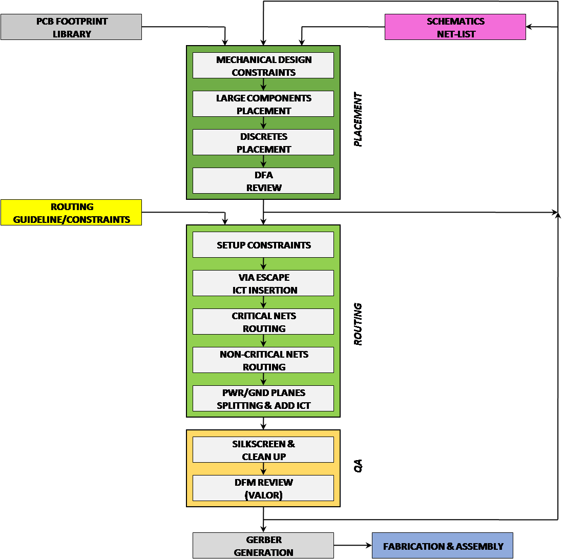
PTEC Solutions Inc. has an ECAD team with strong experience to offer the best PCB Design and Layout service at competitive prices and with extremely quick turnaround time. We have been praised by many customers to be the best CAD Design team they have worked with.
⇒ Have completed designs that could not be completed by other layout companies
⇒ Referred by many US customers as the best team that can handle efficiently direct interface between US & oversea VN/low cost team
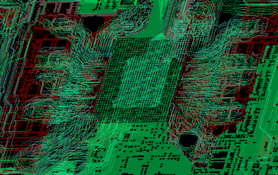
⇒ Smart strategy/planning allowed 100% manual routing at very fast pace – No AutoRoute allowed
- Design Capabilities
⇒ High Speed Digital, Analog, Mixed & RF designs
⇒ Flexible PCB & Rigid-Flex PCB
⇒ High Density PCBs with via in pad technology
⇒ PCB Library management
⇒ Routing constraint management
⇒ DFA/DFT/DFM verification
- Team Experience
⇒ Complete many complex PCB layout:
» 90% of these boards have 24+ layers; 5K to 20K components; 3K to 13K nets
» DDR2/DDR3/DDR4, PCIe, SGMII, USB…etc
» SAS, SATA Gen1/2/3
» XAUI, XFP, SFP, SFP+, Backplane SERDES, QPI
» High current density power rails
» Back Drilled Via Technology
» Blind/Buried Via Technology
⇒ Precise layout estimation schedule
⇒ Study feasibility of placement and routing and propose full solutions of PCB size & stack-up
⇒ Identifying & correcting errors/mistakes by customers including schematic errors
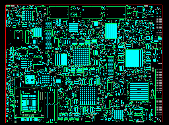
» Board size: 19” x 14”
» Layers: 28
» Thickness: 0.128”
» Total components: 14,000
» Total nets: 10,000
» Back-drilling: YES
» High current density power rails: 90 Amps